Designing your PCB with best practices in place is essential for creating a reliable device at an affordable price.
While the components and materials matter, make sure you leave yourself time in the design phase to think about and utilize the printed circuit board layout.
A well-designed PCB layout means your product has a high potential to make it to the market.
On the other hand, a poorly designed PCB can lead to electronic interference, limited board functionality, and overall component or board failure.
To take your printed circuit board’s design to the next level and ensure it makes it to final production, here are a few steps to follow and considerations to take when designing and laying out your PCB.
General PCB Design Steps
To begin, let’s start with the general steps included in the printed circuit board design process.
Conceptualize
This initial step will help determine what the purpose of your PCB is.
What is the intended outcome? What components will it need to function correctly?
Here, you will take the long-term considerations into play, like what temperature it will need to operate at, what features it will have, and what the board dimensions and placement of components will be — then, you’ll draw out the schematics.
Draw Out the Schematics 
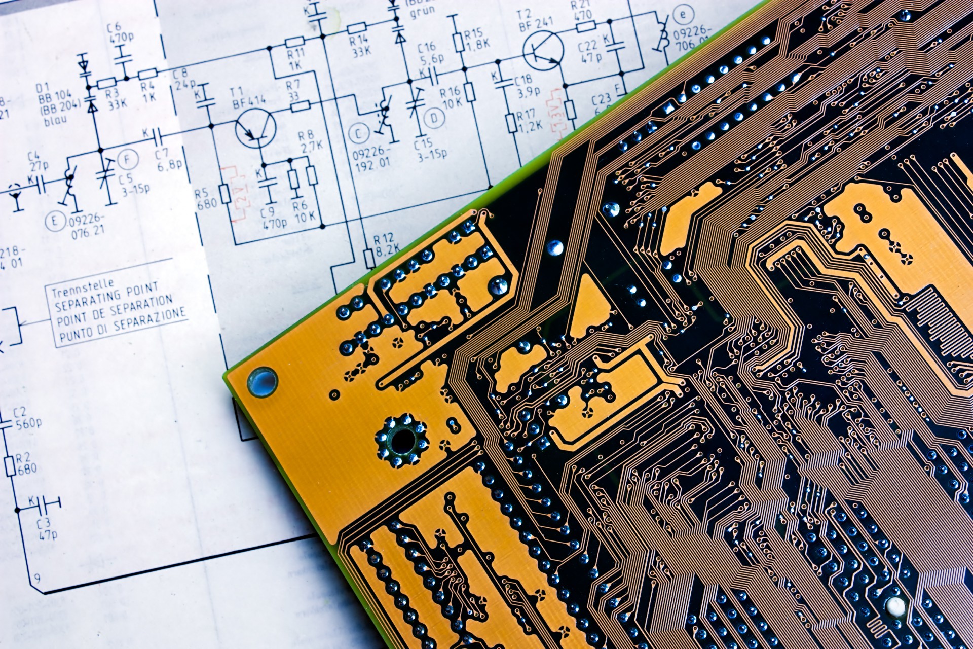
The next phase is to draw out your schematic diagram for your project.
A schematic diagram will include all of the components you need for your project and the component details. Component details have names, part numbers, ratings, and values.
While you create your schematics, you’ll also be developing your bill of materials (BOM). A BOM is used to list all the components for your board. The BOM and the schematics need to be updated in tandem.
Create Your Board-Level Block Diagram
A board-level block diagram will describe and document the precise final dimensions of your board.
Each area on the diagram should be marked for blocks, components, and constraints.
Determine Your Component Placement
This stage of the design process determines where each component will go on your board.
Try to keep components close together to keep traces short.
You will most likely have many stages of working through the component placement, so don’t get discouraged — this is common. It takes time to ensure that every component is placed in the best possible location to maximize your printed circuit board’s quality.
Establish the Circuit Routing
Finally, you will determine the priority of your circuit routing.
Establishing the circuit routing puts the step of placement into action by determining each active element’s location.
PCB Design and Layout Considerations
Now that you have a better idea of how the PCB design process works, it’s important to consider the following factors before starting on the design production of your PCB.
Manufacturing Process
There are many factors to consider and prep that needs to be done in order for manufacturing to begin.
As an overview, consider the limitations and strategies of the board you’re trying to design.
Having an efficient manufacturing process from the get-go will help maximize your company’s electronic device production.
A few things to keep in mind when designing are to keep components away from PCB holes, determine the mounting method that’s best for your product, and decide on the type of materials to be used.
When you’ve figured out your specs, interview a few manufactures — make sure to talk to them thoroughly about their capabilities and potential downfalls. If you feel that a manufacturer is not truthful about their abilities or tolerances, move on. You will be able to find one that meets your needs and requirements.
Board Restrictions
It’s no secret that as technology advances and consumer needs change, printed circuit boards are becoming more complex, small, and sophisticated.
With these changes in design come hurdles as well.
When designing your printed circuit boards, consider the board restrictions. Factors to mull over are the size, shape, and number of power levels.
The functionality and size of your final product will determine your board’s size when you’re designing the layout.
As for shape, the majority of PCBs are square or rectangular. It is possible to design other shapes, but this isn’t a common method, so it comes with high risks and higher costs.
To determine the number of power levels needed, you have to consider whether a complex board for your electronics’ advanced functionality is required. Understand that the more complex a board is, the more it will cost to produce.
 Components and Materials Considerations
Before purchasing materials and components, do your research.
When conducting this research, determine if the required resources are accessible and available at the right price for your budget. Many things can tweak the cost of goods, like using multi-layer boards or adding solder masking to your final product.
Make you don’t rush this stage of the process. You want materials that complement each other’s strengths and weaknesses to ensure the highest quality functionality for your devices. It’s also essential to make sure each component can fit alongside the others without causing any issues in layout or functionality.
Component Sequence of Placement
Not to be confused with component placement, your board placement sequence is when you determine the order that you would like your components to be placed on your board.
Most printed circuit board manufacturers add connectors first, followed by precision circuits, critical circuits, and then the remainder of the elements.
When you’re working in this stage, consider routing and generation capabilities, power levels, routing priority, and power levels.
If you don’t take all considerations into your design process early on, you might end up with conflicting circuit paths or components. When this happens, you’ll have to go back to the drawing board.
Placement Location
The location placement of your components affects performance, testing, functionality, and repair accessibility.
The placement of components can make or break your final product. There are specific ways to place components to get the planned result efficiently.
Remember that placing your components too close will take out the ability to automate the placement — this will slow down testing. When components are too close to the board, machines or engineers must be ultra-careful when placing, touching, reworking, or testing any board. It also takes more time in production; engineers are required to operate slowly and carefully.
A best practice is to leave at least 100 mils between components and the PCB’s edge.
To help prevent any potential placement issues of your PCB components, keep in contact with your manufacturer. A PCB manufacturer should act as a helpful hand when needed and guide you in the right direction to help you create the most efficient end-product.
Orientation and Organization
All of the components on your board should be facing the same direction to prevent confusion during the manufacturing process, specifically in the soldering process.
To avoid any confusion, try to organize your components in this way to increase efficiency while reducing the steps for assembly and reducing cost.
The Importance of PCB Testing
Once you’ve worked through the considerations and factors above, you will be ready to start the process of designing and laying out your printed circuit board.
While these steps are meant to reduce inefficiencies and errors, nothing is guaranteed — especially for novice designers. Keep in mind that there will always be some trial and error in designing. The goal is to limit errors as much as possible.
If you don’t have a team to test your final product, it’s important to make sure your PCB manufacturer tests it to ensure your electronics are ready to go to market.
