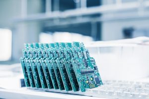
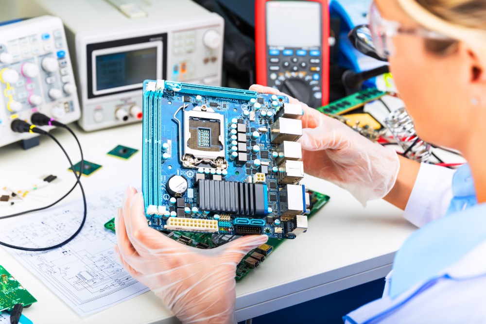
In the world of electronics, the printed circuit board (PCB) is ubiquitous. They come in several sizes and shapes, and they control how the device works. For many, the PCB looks like a small map, or a piece of modern art, rather than the brain of a high-tech device.
To make this intricate piece of technology, manufacturers have to follow several elaborate steps.
What is a PCB?
A printed circuit board is a necessary component in any piece of technology. The PCB connects the electronics by giving them a path to communicate. To make the board fit into a compact area, the board usually has interconnecting layers that are pressed together.
Some PCBs can have 30 or more layers!
The board has conductive elements etched onto a non-conductive material. It was first designed in the 1920s but did not reach commercial production until the 1940s.
How is a PCB Manufactured?
To make a printed circuit board, manufacturers use several of the same generic steps that other intricate products use. But, the PCB has a few extra steps.
Step 1: Designing the PCB
Once a customer places an order, the manufacturer, designer, and customer work together to create a design. The time it takes from order to final design varies as manufacturers use different methods.
Eventually, the design needs to have step-by-step instructions for the particular PCB. The files are reviewed and prepared. Then, with a trace width calculator, manufactures can deduce the details for the inner and outer layers.
Step 2: Printing the Design 
Once the manufacturer and customer have approved the design, the next step is preparing the map. Printing the design helps the manufacturer see what each layer needs.
Manufacturers use a laser plotted printer that uses clear ink to show non-conductive areas and black ink for the conductive areas which will be made of copper traces and circuits. The plotted printer prepares a film so the details of each layer are easy to recognize.
Step 3: Creating the Substrate
The first PCB manufacturing step is to create a substrate that will house the components. The substrate is non-conductive and insulates the components. It’s placed in an oven to be semi-cured, then copper is pre-bonded to both sides of each layer.
The copper is etched to replicate the design from the printed films. At this point, the PCB we are familiar with starts to take form.
Step 4: Printing the Internal Layers
The internal layers are the next part of the PCB that gets attention. Manufacturers use an automated optical inspection (AOI) to carefully assess each layer of a multilayer PCB prior to laminating them.
The design is printed onto the body of the structure, which is also called the laminate.
After the design is printed, a photo-sensitive film made from photo-reactive chemicals covers the laminate. The photo-reactive film hardens when it is exposed to light. The film helps the manufacturer align the blueprints onto the board.
Once the film hardens:
The manufacturer drills several holes into the PCB to align the layers.
Step 5: Using Ultraviolet Light
When the holes are alighted, manufacturers place the resist and laminate under UV lights to further harden the structure. The resist is a permanent resin coating that gives the PCB its green coloring.
After the board is hardened, light shows manufacturers where the copper pathways go. The black ink from step 2 does not harden and is removed later in the process. After the resist and laminate are hardened, the board is placed into an alkaline solution to remove any leftover resist.
Step 6: Removing Unwanted Copper
During production, there will be unnecessary remnants of copper on the board. Manufacturers use a chemical solution to remove unwanted copper. The solution breaks down the metal, but the photoresist stays intact.

Step 7: Inspecting the Layers
As the PCB involves precise alignment, manufacturers need to inspect projects regularly. After the copper is removed, the layers need to be inspected for alignment. An optical punch machine drills a pin through the holes to ensure the layers are properly aligned.
This is the last inspection step, so another machine looks for other defects. Anything after this step cannot be corrected, as the PCB foundation is completed.
Step 8: Laminating the Layers
If the board passes inspection, then the next step involves laminating the layers. An epoxy resin layer is placed in the alignment basin. That resin is called a prepreg, and the next step involves covering it with a layer of substrate.
Copper foil is added next. Then more prepreg and another copper layer.
Step 9: Pressing the Layers
When the layers are aligned and ready, the PCB manufacturer uses a mechanical press that applies heat and pressure. The epoxy in the prepreg layer melts to fuse the layers.
Step 10: Drilling the Layers
After the layers are pressed, the next step involves more drilling. These drill holes expose the substrate and inner panels. The computer-guided drill works with two or three panels simultaneously.
Step 11: Plating the PCB
When the drill holes are in place, the layers are plated with a chemical solution that fuses them together. During this process, the PCB is cleaned thoroughly with several chemicals.
Eventually, manufacturers coat the panel with a layer of thin copper, which is only 45 to 60 millionths of an inch in thickness.
Step 12: Imaging the Outer Layer
After the plating process, manufacturers apply a player of photoresist (similar to what is applied in Step 3) before imaging happens. UV light is used to harden the photoresist, and any extra photoresist is removed before another layer of plating is applied.

Step 13: Plating the Panel
Manufacturers apply another layer of thin copper to the panel. Then apply a thin layer of tin guard, which keeps the copper protected so it’s not etched off during the next step.
Step 14: Etching the Connections
Manufacturers remove any excess copper using a chemical solution. The protective tin layer keeps the necessary copper in place. At this point, the PCB connections are established.
Step 15: Applying the Solder Mask and Legend
After all of the plating and removal of excessive metal, the panels are all cleaned before another layer of epoxy with a solder mask is applied. At this stage, the solder mask turns the board green.
Then:
The manufacturer uses silkscreening to print the important parts of the board for reference during the next steps.
Step 16: Surface Finish
This is the last production stage before testing. During this step, a final chemical process is applied to finish the surface. Manufacturers have several finishing products to choose from, but most choose Hot Air Solder Level (HASL).
Other choices include:
- Electroless Nickel Immersion Gold (ENIG)
- Soft or Hard Gold
- Immersion Tin or Silver
- Organic Solderability Preservative (OSP)
Step 17: Testing the PCB
The PCB isn’t complete until it passes a final test. A technician performs an electrical test. The technician confirms that the PCB functions and follows the original blueprint designs.
With 17 precise steps, manufacturing a PCB is a lengthy and complicated process that uses a variety of materials. If you need a high-quality PCB, consider outsourcing the process to a contract manufacturer, as they have the technical expertise and cost-effective manufacturing methods.
