Soldering is an essential activity in electronics assembly; it’s used in the electronics industry to join pieces of printed circuit boards (PCBs).
Soldering is important in building any electrical equipment or item, from a small child’s toy to huge refrigerators. Although the procedure seems straightforward, even a tiny error or imperfection in soldering can lead to malfunctions in the PCB. The quality of soldering directly affects the output of the PCB.
There are many electrical parts connected to the PCB, including resistors, capacitors, transistors, and LEDs. Joining these parts together makes the device function as it ought to, but improper soldering might result in these parts jostling around. This can lead to a poorly functioning, unreliable gadget or piece of electronic equipment.
Improper soldering has serious repercussions for many parties — from electronics manufacturers to retailers — but especially for consumers. A poor soldering job could lead to:
- A loss of profit for manufacturers because distributors may request refunds for poorly produced electronics
- A bad reputation and loss of market credibility for manufacturers
- A loss of customers for retailers and distributors who sell the dysfunctional product
- Problems such as fires, damaged equipment, and more for consumers who buy the products
This is why industry experts put soldering at the top of their list for heavy scrutiny and assessment in order to determine the quality of a device.
Common Soldering Problems
To avoid the dangerous repercussions of poor soldering, we have created a list of common soldering issues to avoid in electronics assembly.
Joint Defects
When soldered appropriately, a perfect solder joint should have a complete, solid wetting, a smooth, shiny surface, and a neat concave filet. When a joint is not properly soldered, it results in one of the following joint defects:
- Disturbed Joint: A disturbed joint occurs when the joint has been moved during the soldering process before it is fully solidified. You can easily spot this because the joint appears rough or frosted. To repair this, reheat the joint and then allow it to cool appropriately.
- Bulbous Joint: A bulbous joint is caused when you solder on a chip component that exceeds the height of the convex meniscus area of the PCB. It usually occurs when there’s a separation of the board from a solder wave.
- Cracked Joint: Cracked joints are usually caused by the thermal expansion of a joint. It often occurs due to the original product design.
- Solder-Starved Joint: Solder starvation is what it sounds like — there wasn’t an adequate amount of solder available to create a perfectly-shaped solder joint. The consequences of this defect include weak solder joint strength, solder joints that are prone to opening, intermittent short circuits, and more.
- Cold Joints: Sometimes in soldering, the solder may fail to completely melt and form a proper joint; the result is what is known as a cold joint. Joints like this are not reliable and may develop even more cracks along the way.
- Incomplete Joint: Incomplete joints occur as a result of poor hole-to-lead ratio, extreme wave temperature, poorly angled conveyors, or contamination at the pad’s edges.
- Overheated Joint: This defect is caused when the solder hasn’t properly flowed, perhaps because the pad contains an existing layer of oxide which prevents heat transfer. It could also result from setting the soldering iron at an extremely high temperature.
Solder Bridges
Manufacturers make PCBs and other electronic components smaller by the day, such that it becomes challenging to manipulate around the PCB during soldering. The small size of the modern PCB makes it extremely important to use properly sized tools for soldering.
Soldering with an extra-large solder iron tip can result in unwanted solder bridges. A solder bridge happens when the material you’re using to solder joins two or more PCB connectors, which could be quite disastrous and even dangerous. If you don’t notice this error quickly, it could result in a short circuit or burnout.
Untrimmed Leads 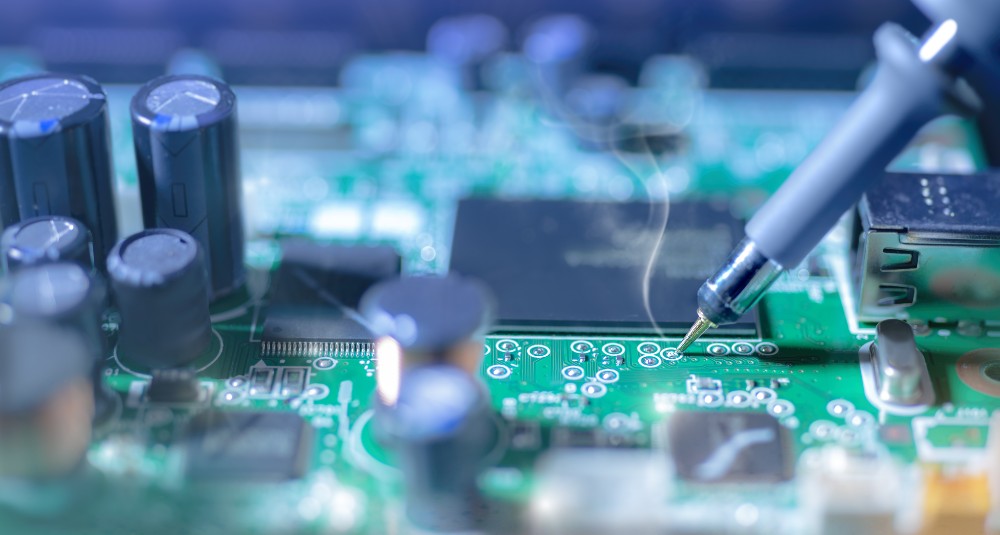
During the soldering process, you may need to use leads for part of the electronics assembly. One small error — leaving your lead untrimmed — can result in short circuits and possibly other damages.
Because of their length, untrimmed leads can easily come into contact with other leads on the PCB. It doesn’t matter if it is just one lead that is left untrimmed. It can adjust or bend to cause a lot of problems in the future.
Too Much Solder
If you’re new to soldering, it can be difficult to judge the amount of solder you need. Using too much solder can cause a large bubble to form around the solder joint, making it disproportionate to the rest of the PCB.
Too much solder can sometimes be difficult to notice, especially if the PCB appears to be working well. You can avoid excessive solder by using just a little at a time, and then adding more if necessary.
Solder Balling
Solder balling occurs frequently with a wave or reflow soldering. It typically looks like a small piece of solder that latches onto a laminate or conductor surface.
Solder balls are often caused when the moisture close to the holes on the PCB turns into steam due to heat. Water vapor moves through these holes or gaps. If there is solder in the hole, it extrudes it and forms solder balls on the PCB.
Lifted Components and Pads
Pad lifting occurs mostly on single-sided boards. After you have done the wave soldering, the heated surface can reduce copper adhesion, causing the components or pads to lift if you apply even the slightest force.
To avoid this, you need to consider thermal and physical factors. If you apply more heat as you wave solder, you have to take care as you handle the printed circuit boards. This is what results in components and pads being lifted or coming loose.
Be careful as you lift off your boards out of pallets or conveyors, and try not to use components of the board as handles.
Tombstones
A defect called a tombstone can occur when you connect transistors and capacitors to your PCB. If done appropriately, the component should be straight, but if you make a mistake with the soldering temperature, some sides may lift, causing it to look like a tombstone.
The uneven heating that occurs in the reflow oven causing premature wetting of the solder on the PCB is the main factor behind tombstones. When a tombstone defect occurs, the solder joint won’t last; it may also negatively impact the thermal performance of the PCB. Uneven heating usually takes place in homemade reflow ovens, which is why it’s advisable to use professional soldering equipment instead.
How To Ensure Proper Soldering
There are many other soldering issues we have not addressed in this article — these are simply the most common ones people fall victim to. Each one can lead to dire repercussions for manufacturers and end-users of the product, so it’s critical that you avoid any mistakes.
Improper soldering can lead to profit loss, customer loss, and even property loss in the case of short circuits or fires. You can avoid poorly soldered products when you work with an established electronics manufacturer. If you intend to hire an EMS provider, these are some of the things to look for in a partner.