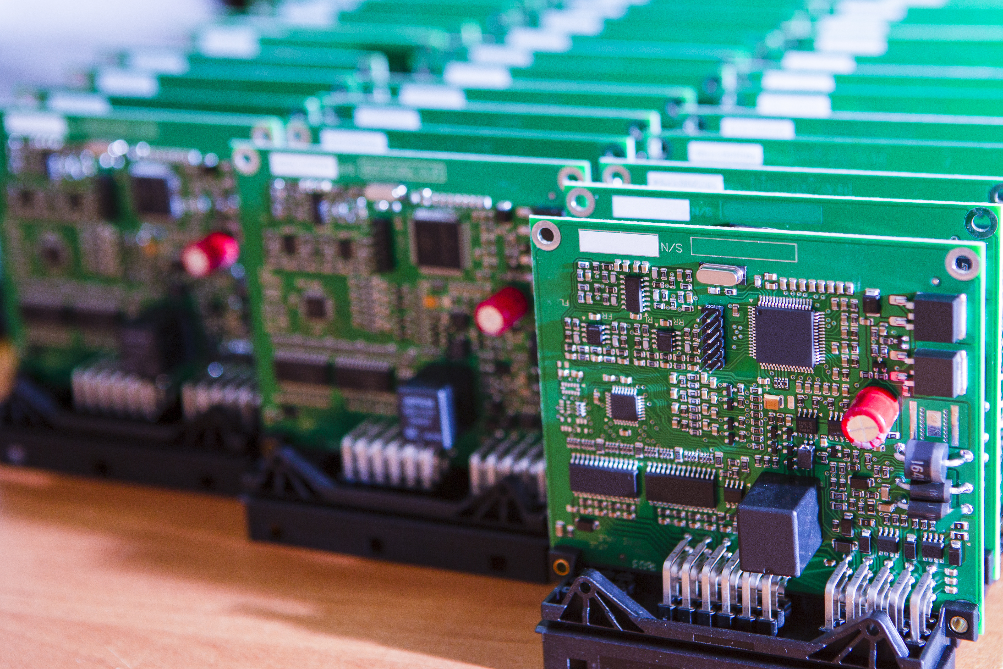
The benefits of PCB plating ensure that the PCB’s surface is well-protected against environmental factors while also providing a smooth and level finish for vias and traces to be laid down on.
Plating also increases the structural integrity of the PCB, making it less likely to flex or warp over time. You can use several different types of plating on PCBs, each with its advantages and disadvantages.
By understanding the basics of PCB plating, you can make an informed decision about the right plating process for your next project and guarantee a reliable, high-quality PCB for any application.
The PCB Plating Process
The steps involved in PCB plating ensure that the board is durable and free from costly manufacturing errors that increase the time to market for a product.
Step 1: Pre-treatment
Pre-treatment is essential to the success of the plating process and ensures that the surface is free from contaminants that could cause defects in the final product. This four-step process includes:
- Deburring. Deburring removes any hole drilling residues, sharp edges, and imperfections from the PCB that could cause plating defects.
- Alkaline greasing. Alkaline greasing removes oils, fingerprints, and other contaminants from the PCB surface built up due to the pre-plating manufacturing process.
- Desmear. Desmear is an epoxy resin etching process using potassium permanganate. This process increases the capacity for absorption of hole walls for better adhesion.
- Micro-etching. Micro-etching roughens the surface of the PCB to provide better adhesion for the plating solution and decrease the risk of delamination.
Step 2: Activation
With factors such as pH, moisture, and oxidation significantly affecting the efficacy of the plating process, activation is key to ensuring a successful outcome. Activation creates an environment on the surface of the PCB that is conducive to the plating. There are a few different activation processes, with the most common being tank submersion to deposit a layer of colloidal palladium that acts as a catalyst for the plating process.
Step 3: Electroless Copper Plating
For hole walls to maintain optimal electrical conductivity and attach to interlayer circuits, it is necessary to plate copper onto the exposed hole walls. You can perform this process using an electroless chemical bath that provides a controlled environment for plating to take place.
Step 4: Panel Plating
The next step is to plant copper onto the exposed surfaces of the PCB. You can take this action using either an electrolytic or electroless chemical bath. Electrolytic plating is the most common method as it offers more control over the process and produces a more consistent outcome.
Different Types of PCB Plating
The type of plating chosen will be based on the requirements of the project and the desired result. Each has its advantages and disadvantages that you should consider before making a final decision.
Through-Hole Plating
PCB through-hole plating is the deposition of electroless copper plating onto the walls of drilled holes and is essential in the manufacturing drilling process. This type of plating protects the circuitry from environmental and chemical damage while also providing electrical connectivity between different layers of the PCB. The advantages of through-hole plating include:
- Increased durability
- Improved electrical connectivity
- Excellent adhesion capabilities
- Reduced chemical treatments
This plating technique is ideal for prototype and small-scale production runs as it is a simple process that does not require specialized equipment or multiple applications.
Brush/Selective Plating
Used primarily in electronics shops when repairing waste boards, brush plating applies a conductive metal to exposed circuitry using a brush. This process allows the repairman or manufacturer to select the areas that need to be plated without completely submerging the board in a chemical bath. The advantages of brush plating include:
- Improved accuracy
- Reduced material cost
- Minimized environmental impact
- Elimination of process waste
This type of plating is ideal for small-scale production runs or when working with boards that have already been populated but need minor repairs on areas such as edge connectors. For brush plating to be successful, you must use a conductive metal solution such as graphite and an absorbent material such as cotton.
Reel Linkage Selective Plating
Pins, integrated circuits, connectors, transistors, and other electronic components are usually plated using reel linkage selective plating. This plating technique allows for the selective deposition of metal onto these components without needing to remove them from the board. The advantages of reel linkage selective plating include:
- Improved accuracy
- Allows for batch welding
- Reduced cycle time
- Oxidation and corrosion protection
This process is typically used in large-scale production runs where there is a need for increased efficiency and reduced waste. Additionally, reel linkage selective plating is often used during the salvage or repair of mismatched parts.
PCB Plating Finishes
The project’s requirements will determine the particular finish used in PCB plating. Choosing the right finish will ensure optimal electrical and mechanical performance. The most common finishes used in PCB plating are:
- Electroless Nickel Immersion Gold (ENIG). This popular PCB plating finish offers the benefits of both nickel and gold. It provides excellent electrical connectivity and is resistant to tarnishing and corrosion. ENIG is typically used in applications requiring fine pitch, easy solderability, and long shelf life.
- Hot Air Solder Leveling. Hot air solder leveling (HASL) is a process that uses heat and solder to level the surface of the board. This type of finish is typically used in applications needing reworking, low cost, and good solderability.
- Immersion Silver. Immersion silver provides excellent electrical connectivity and is RoHS- certified. Immersion silver is often used in high-frequency applications where a fine pitch is required. The silver plating is deposited using a chemical process.
- Organic. Organic water-based surface finishes are typically used in applications where there is a need for low loss of frequency, fine pitch, and lead-free compliance. These finishes are easier to apply than other finishes and are typically used on boards that will not be exposed to harsh environments.
- Hard Gold. Similar to ENIG plating but with more thickness, gold plating provides excellent electrical connectivity and is durable. Hard gold is typically used in applications such as keypads, edge connectors, and molded interconnect devices.
- Carbon Ink. Carbon ink plating is very suitable for applications stationed in tropical regions. It provides an affordable alternative to hard gold plating, especially when the need for a very thick gold coating is not required.
- Electroplating. Electroplating is the process of depositing a thin layer of metal onto a conductive surface. This process is often used to improve the surface’s solderability, conductivity, or wear resistance. Electroplating is typically used in through-hole vias and surface traces.
Properly Plate Your PCB
The importance of choosing the best PCB plating material and method cannot be overstated. Properly plated PCBs will ensure optimal electrical and mechanical performance while protecting against environmental damage. Additionally, choosing the best PCB plating solutions will ensure no issues throughout the entire development and manufacturing process.
With the many finishes and plating techniques available, it is always important to consult a qualified PCB manufacturer to determine the best solution for PCB plating.