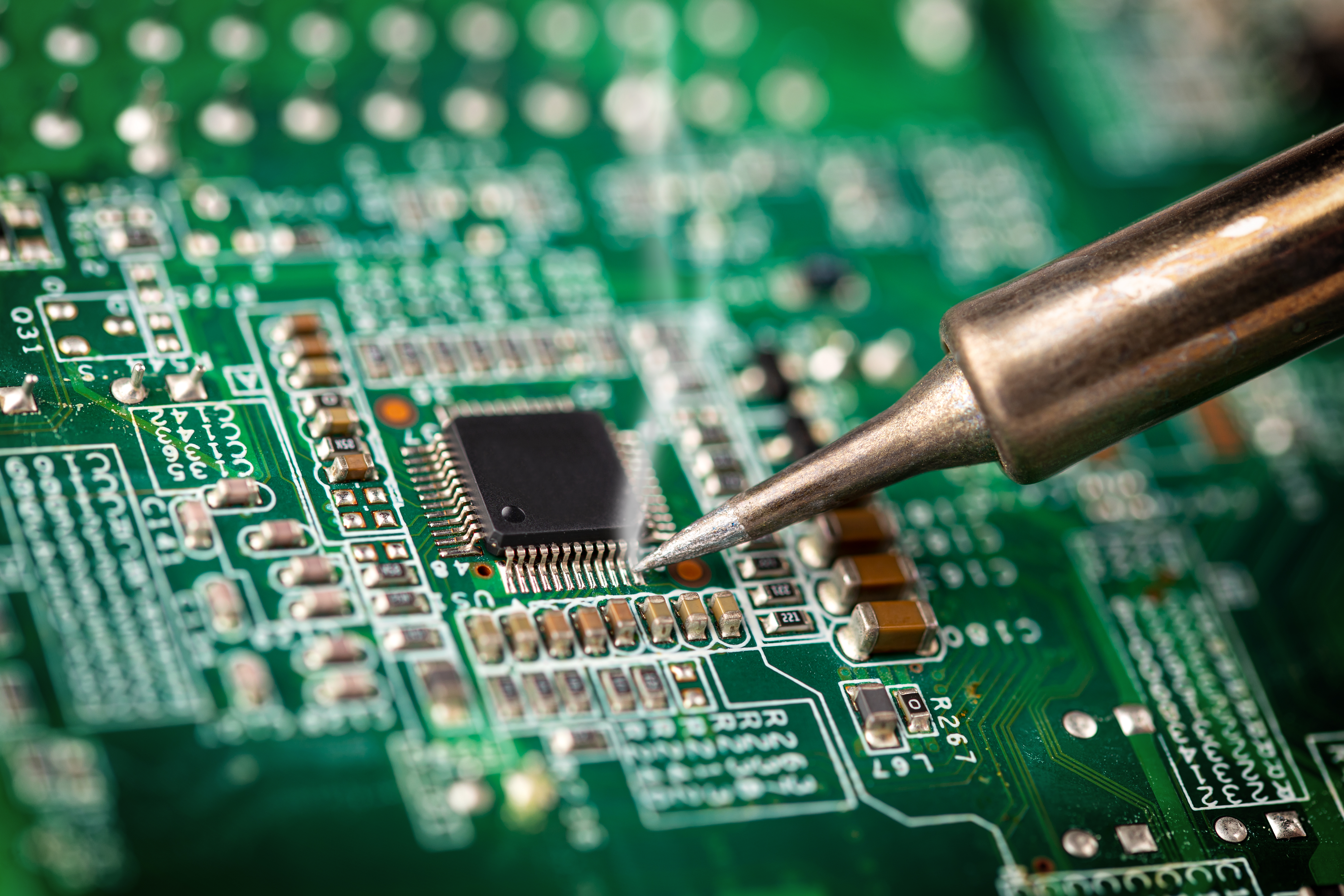
PCBs are intricately designed, with hundreds of joints and components requiring soldering to create functioning electrical connections. Unfortunately, soldering mistakes can lead to costly repairs or even complete PCB replacement. Considering the importance of PCBs in the modern digital world, it’s essential to ensure that they are soldered correctly to avoid poor function or increased overhead.
To ensure that your PCB boards are free from soldering errors that would affect the performance of the PCB, it’s essential to avoid making these most common PCB soldering mistakes.
Using Excessive Soldering
One of the most common mistakes made by inexperienced PCB manufacturers is using excessive soldering. Excessive soldering happens when too much solder is applied to the pin, resulting in a soldered joint that is taller or more rounded than the surrounding component leads.
Not only is this excessive soldering unsightly, it can also lead to other issues such as:
- Short circuits
- Poor electrical connections
- Difficulties in desoldering
- Problems finding soldering joint
Excessive soldering issues can be easily avoided by properly wetting, heating, and applying the solder. When in doubt, remember that less is more when soldering PCB components.
Unwanted Soldering Bridges
Most commonly caused when using a soldering tool too big for the PCB job, soldering bridges occur when two separate PCB tracks or component leads are accidentally connected by a haphazard or excessive amount of solder.
Not only can solder bridges cause a short circuit, but they can also make it difficult to remove and replace components as needed. To avoid unwanted soldering bridges, use a soldering tip that is the appropriate size for the PCB tracks and components being soldered.
If a solder bridge does happen, it can usually be removed by melting the middle of the bridge with a soldering iron and drawing the excess solder away with a desoldering tool.
Joint Errors
Joints are essential to the overall PCB performance, so it’s crucial to ensure that they are properly made. Well-made PCB joints will have a glossy, wet look and should be shiny. Anything outside of these parameters is considered a joint error. The two most common joint errors are cold joints and burnt joints.
Cold joints are those that didn’t reach the proper soldering temperature and, as a result, are not as strong as they should be. Cold solder joints resemble a dull, frosted, or flaky matte finish and can be easily broken. To avoid cold solder joint errors, use a higher soldering temperature.
Characterized by a dull, black appearance, burnt joints occur when too much heat is applied to the PCB during the soldering process. This soldering mistake can cause the PCB tracks to lift and damage the PCB and components. Avoid overheating PCB joints by lowering the current soldering temperature and using a good PCB design that can handle thermal stresses.
Skips
Solder skips happen when the solder fails to adhere to the PCB track or component lead and can be identified by the recessed, sunken appearance of the PCB track or component lead on one or both sides of the PCB. Skips will cause an electrical open circuit, resulting in signal loss or PCB failure. PCB solder skips can be caused by several factors such as:
- Dirty PCB tracks or leads
- Insufficient soldering temperature
- Use of incorrect solder type
- Human or automation error
PCB solder skips can usually be fixed by applying additional solder to the affected area. However, if too much time has passed between PCB fabrication and soldering, it may be necessary to scrape away the old solder and start fresh.
Lifted Pads
Solder pads are small copper areas on a PCB that provide an electrical connection between the PCB and its components. If too much heat is applied during soldering, these solder pads can lift away from the PCB, taking the component lead along with it. Pads can also lift when excessive force or torque is applied to PCB components during assembly or repair.
Correcting lifted pads can be tricky but not impossible. If the lifting is minor, there is a good chance it can be fixed by reattaching and resoldering the pads. However, if the lifting is severe, it may be necessary to replace the entire PCB. To avoid this issue altogether, use caution when applying heat and force to PCBs during assembly and repair.
Tombstoning
Aptly named for the hallmark graveyard marker, tombstoning occurs when a component is mounted on a PCB, but only one lead is soldered to the PCB, thus giving it a tilted tombstone-like appearance. Tombstoning has many causes, including:
- Incorrect PCB design
- Human error
- Thermal stresses during the soldering process
To avoid tombstoning, use a good PCB design and follow the correct assembly and soldering procedures. It is also imperative that the engineer designing the PCB account for solder wave direction to prevent tombstoning from occurring from the get-go.
Fortunately, if tombstoning does occur, it can usually be fixed by reheating the solder joint and repositioning the component. However, the PCB may need to be reworked entirely in some cases, especially if the tombstoning is severe.
Poor Wetting
Proper wetting is essential for making strong, reliable solder joints free from gaps, voids, or pinholes. Poor wetting can be caused by many factors, including:
- Dirty or poorly designed PCB tracks or leads
- Insufficient soldering temperature
- Use of incorrect solder type
- Solder that is too old or has been stored improperly
- PCB design errors
To avoid poor wetting, clean PCB tracks and leads before soldering. Also, always remember to use a solder appropriate for the application.
Avoid PCB Soldering Mistakes
There is a lot that can go wrong when soldering PCBs. To avoid costly mistakes, always use the proper soldering techniques and materials. Additionally, it’s vital to ensure that the PCB is designed with suitable materials to handle the thermal stresses of soldering. If you need help to prevent these or any other common PCB soldering mistakes, consider looking for an EMS partner with experience in PCB design and fabrication.