PCB lamination is among the many crucial steps required to create a high-quality printed circuit board. Without lamination, a PCB would be too fragile to function properly — ruining the circuitry and making the board unusable.
Knowing which PCB lamination process is best for a particular application is critical to ensuring that the product functions exactly as needed. Check out the different PCB lamination processes and what factors you need to consider when choosing one.
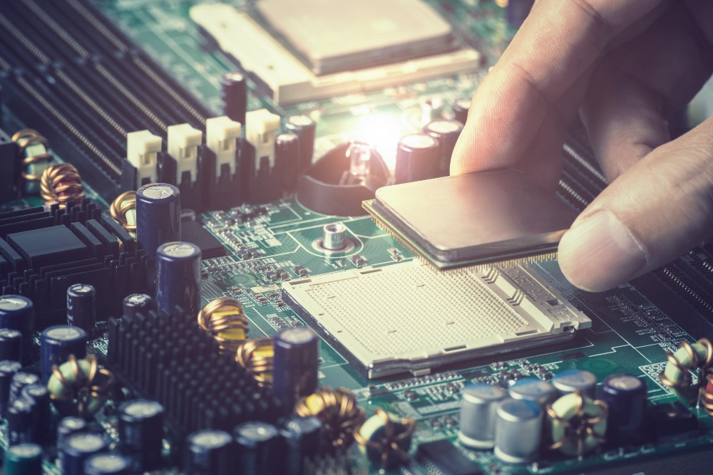
Types of PCB Lamination
The best PCB lamination process will depend on the application of the PCB in addition to its size, complexity, and layer count. Choosing the right method will improve product reliability, decrease layer-to-layer registration, and minimize warpage.
Multilayer PCB Lamination
Multilayer PCB lamination uses heat and pressure on prepreg material to bond layers together. The prepreg material is typically made from glass fiber or paper infused with a thermosetting resin. This type of lamination is often used for boards with four or more layers. It offers several advantages, including:
- Good dimensional stability
- Excellent layer-to-layer registration
- High reliability
The process involves placing prepreg material between the layers of the PCB, then heating the entire stack under intense pressure until the prepreg material cures and bonds the layers together. Once a strong bond has been formed, pressure is slowly released as the PCB cools off, ensuring no deformation occurs.
While a slower and more complex process than other types of PCB lamination, multilayer lamination offers superior results in terms of product reliability. It’s also the best chance to make sure that complex circuitry functions as intended in electronics, medical devices, and aerospace applications.
Sequential PCB Lamination
Sequential lamination is the best choice when bonding two to four substrates. Sequential lamination involves a step-by-step process that builds up the layers of the board one at a time. This process is done by adding and curing layers of dielectric material and copper until the desired board thickness is achieved. This type of lamination offers many benefits, including:
- The ability to fine-tune the properties of each layer
- Improved dimensional stability
- Low warpage
- Excellent layer-to-layer registration
This type of lamination is typically used for PCB boards where stability and precision are critical to optimal machine performance, such as in military or aerospace applications. It’s also a good choice for boards with complex features, such as blind or buried vias.
Teflon (PTFE) Microwave Lamination
Creating PCBs for radio frequency (RF) and microwave applications requires using Teflon, also known as polytetrafluoroethylene (PTFE). Teflon has good dimensional stability, can withstand extreme temperatures, is an excellent electrical insulator, and is resistant to moisture and heat, making it ideal for use in high-frequency applications. The Teflon microwave lamination process offers many benefits, including:
- High signal speed
- Minimal connection interruption
- Tight depth tolerance
- Excellent dimensional stability
This lamination process is distinctive because it uses thermoplastic film (chlorotrifluoroethylene) rather than a photo-resistant one. This feature allows for better protection of the inner layers of the PCB.
Those needing to create RF and microwave PCBs will find that Teflon microwave lamination is the best way to achieve the desired results. Additionally, this lamination process may be the only option for military applications or purposes due to the stringent requirements for military-grade PCBs.
Double-Sided PCB Lamination
As its name suggests, this lamination type involves bonding two substrates together with a dielectric material in between. Double-sided lamination techniques don’t require the same pressure, making them faster and more affordable than other options like single and multilayer lamination processes. The benefits of double-sided lamination include:
- Reduced costs
- Simplified process
- Faster turnaround time
This type of lamination is typically used for applications that don’t require the use of blind or buried vias, such as in power supplies or general-purpose electronics. Additionally, double-sided lamination is a good choice for those working with smaller boards or prototyping new designs.
Step-By-Step PCB Lamination
While the various specifics of each lamination process vary from one type to another, some general steps are followed in all cases:
- Preparation. Cleaning the substrates, metalization layers, and dielectric material ensures the components are free of any contaminants that could interfere with the bonding process.
- Micro-etching. Once the materials are clean, the next step is to etch micro features into the metalization layers. Taking this action helps make sure that the layers bond together properly.
- Black Oxide Treatment. This step is used to improve the adhesion of the metalization layers to the substrate, avoiding common PCB manufacturing issues such as delamination.
- Inner Layer Stack-Up. The next step is to build the inner layer stack-up. This process involves bonding the layers and prepreg on a gluing machine to ensure inner layers and the prepreg won’t move during cure.
- Stack-Up. The layer creation is completed through the stack-up of copper and dielectric material. The application requirements will determine the number of layers.
- Lamination. The final step is to run the stack-up through a lamination process to bond all the layers together. You can do this step manually or automatically, depending on the size and complexity of the board.
- Hole Registration. After lamination, the next step is to align the drilled holes with the pads on the layers. This is typically done with an X-ray machine. Once holes are marked, you can begin the process of finalizing the PCB.
PCB Laminate Factors to Consider
Material quality and cost will be the two most important factors when choosing a laminate material for your PCB. Power and energy efficiency will also be critical factors in ensuring a PCB’s compatibility with the end-use application. Depending on the application and desired results, other important factors to consider include:
- Glass Transition Temperature (Tg)
- Thermal conductivity (k)
- Coefficient of thermal expansion (CTE)
- Dielectric constant (Dk)
- Surface resistivity (pS)
- Flame retardancy
- Moisture absorption
- Density
- Chemical resistance
- Time to delaminate
Finally, you should take the certifications of a PCB manufacturer and the company’s research and development capabilities into account to guarantee the highest quality product.
Common PCB Lamination Issues
Choosing the wrong lamination process or failing to account for the factors mentioned above can lead to several issues during the PCB manufacturing process, including:
- Blistering. Blistering occurs when too much humidity or heat is present in the lamination process. This issue can cause bubbles and gaps that render the PCB ineffective. Solutions include proper drying of the materials before lamination and using lower temperatures during the process.
- Voiding. A PCB lamination void can occur due to resin gaps between bonding materials, excess moisture on layers prior to lamination, or air pockets between layers. Oven drying or increasing resin pressure are the best solutions for this common occurrence.
Voiding and blistering can lead to delamination that causes the PCB to fail. Therefore, it’s essential to work with a reputable PCB manufacturer using high-quality materials and practices to avoid these issues.
Find Your PCB Manufacturing Process
The PCB lamination process is a critical step in manufacturing printed circuit boards. With the knowledge of selecting the right lamination process and what materials to use, you can avoid common issues during PCB production and create a high-quality product. No matter your PCB lamination needs, choose a PCB manufacturer with the certifications, research and development capabilities, and experience to deliver a world-class product.